Academician Yu Dapeng involved in significant quantum theory paper
2019-05-03
The development of two-dimensional (2D) materials has opened up possibilities for their application in electronics, optoelectronics and photovoltaics, because they can provide devices with smaller size, higher speed and additional functionalities compared with conventional silicon-based devices. The ability to grow large, high-quality single crystals for 2D components—that is, conductors, semiconductors and insulators—is essential for the industrial application of 2D devices.
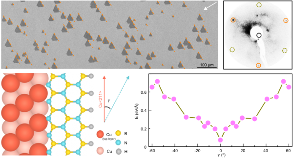
Last week, Dean of the Shenzhen Institute of Quantum Science and Engineering and Chair Professor of the Department of Physics at Southern University of Science and Technology (SUSTech) Yu Dapeng was involved in a significant paper published in Nature, entitled “Epitaxial growth of a 100-square-centimeter single-crystal hexagonal boron nitride monolayer on copper.” Working with Liu Kaihui and Wang Enge from the School of Physics of Peking University, the paper provided the first report on the universal growth mechanism of single-crystal 2D hexagonal boron nitride (hBN) on symmetry broken single-crystal copper substrates. It is expected to be extended to prepare large-area single crystals of other 2D materials.
Atom-layered hBN, with excellent stability, flat surface and large bandgap, has been reported to be the best 2D insulator. However, the size of 2D hBN single crystals is typically limited to be less than one millimeter, mainly because of the difficulties of excessive nucleation which preclude the growth from a single nucleus to large single crystals, and the threefold symmetry of the hBN lattice, which leads to antiparallel domains and twin boundaries on most ordinary substrates.
In 2017, the research team and collaborators reported for the first time the preparation of a meter-scale single-crystal Cu(111) foil and epitaxial growth of meter-scale single crystal graphene on it (Science Bulletin 2017, 62, 1074). Unlike graphene, the lattice of most 2D materials such as hBN are non-centrosymmetric, two preferential domain orientations with rotation angle of 180° exist during epitaxial growth, and the twin grain boundaries would generate when domains get coalesced.

The key to solve this problem is to find a substrate with suitable symmetry. The research team explored a new method to preparing the substrate with non-centrosymmetric surface. Through the patented annealing approaches, the industrial polycrystalline copper foil could be converted into the single-crystal Cu(110) with small-angle inclined, which only has C1 symmetry. The coupling between Cu<211> step edge and zigzag-edge of hBN domain with different termination (B- or N-) has different formation energy, which breaks the equivalence of lattice orientation between hBN domains with rotation angle of 180°. Thereby, unidirectionally aligned hBN domains have been obtained and then seamless stitched into an entire piece of single crystal with large area and high quality. Such method can be extended to the synthesis of large-area single crystal of other 2D materials, and it is also expected to promote the technological development of board applications of new 2D material devices.
Wang Li, Xu Xiaozhi, Zhang Leining, and Qiao Ruixi are the co-first authors of the paper, and Liu Kaihui and others are the communication authors. Qiao Ruixi is a Ph.D. student of Academician Yu Dapeng. Liu Kaihui is a young scholar introduced by Academician Yu Dapeng from the US UC-Berkeley in 2014 to the Nanostructure and Low-dimensional Physics Laboratory of Peking University.
This work was supported by the National Key R&D Program of China, the Natural Science Foundation of China, the National Equipment Program of China, the Beijing Municipal Science & Technology Commission, the Beijing Graphene Innovation Program, the Shenzhen Municipal Science, Technology and Innovation Commission, the Guangdong Innovative and Entrepreneurial Research Team Program, the Industry and Information Technology Bureau of Shenzhen Municipality, the National Postdoctoral Program for Innovative Talents, the Strategic Priority Research Program of CAS, the National Program for Thousand Young Talents of China and the Institute for Basic Science of South Korea.


